- 您现在的位置:买卖IC网 > Sheet目录2005 > LTC2225IUH#TRPBF (Linear Technology)IC ADC 12BIT 10MSPS 3V 32-QFN
LTC2225
12
2225fa
sample-and-hold charging glitches and limiting the
wideband noise at the converter input.
APPLICATIO S I FOR ATIO
WU
UU
The difference amplifier generates the high and low refer-
ence for the ADC. High speed switching circuits are
connected to these outputs and they must be externally
bypassed. Each output has two pins. The multiple output
pins are needed to reduce package inductance. Bypass
capacitors must be connected as shown in Figure 6.
Other voltage ranges in-between the pin selectable ranges
can be programmed with two external resistors as shown
in Figure 7. An external reference can be used by applying
its output directly or through a resistor divider to SENSE.
Figure 5. Single-Ended Drive
Figure 4. Differential Drive with an Amplifier
25
25
12pF
2.2
F
VCM
LTC2225
2225 F04
–
+
CM
ANALOG
INPUT
HIGH SPEED
DIFFERENTIAL
AMPLIFIER
AIN
+
AIN
–
25
0.1
F
ANALOG
INPUT
VCM
AIN
+
AIN
–
1k
12pF
2225 F05
2.2
F
1k
25
0.1
F
LTC2225
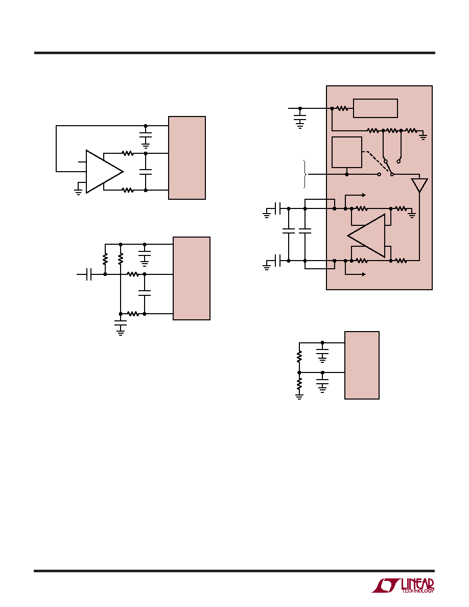
Reference Operation
Figure 6 shows the LTC2225 reference circuitry consisting
of a 1.5V bandgap reference, a difference amplifier and
switching and control circuit. The internal voltage refer-
ence can be configured for two pin selectable input ranges
of 2V (
±1Vdifferential)or1V(±0.5Vdifferential).Tyingthe
SENSE pin to VDD selects the 2V range; tying the SENSE
pin to VCM selects the 1V range.
The 1.5V bandgap reference serves two functions: its
output provides a DC bias point for setting the common
mode voltage of any external input circuitry; additionally,
the reference is used with a difference amplifier to gener-
ate the differential reference levels needed by the internal
ADC circuitry. An external bypass capacitor is required for
the 1.5V reference output, VCM. This provides a high
frequency low impedance path to ground for internal and
external circuitry.
VCM
REFH
SENSE
TIE TO VDD FOR 2V RANGE;
TIE TO VCM FOR 1V RANGE;
RANGE = 2 VSENSE FOR
0.5V < VSENSE < 1V
1.5V
REFL
2.2
F
2.2
F
INTERNAL ADC
HIGH REFERENCE
BUFFER
0.1
F
2225 F06
LTC2225
4
DIFF AMP
1
F
1
F
INTERNAL ADC
LOW REFERENCE
1.5V BANDGAP
REFERENCE
1V
0.5V
RANGE
DETECT
AND
CONTROL
Figure 6. Equivalent Reference Circuit
Figure 7. 1.5V Range ADC
VCM
SENSE
1.5V
0.75V
2.2
F
12k
1
F
12k
2225 F07
LTC2225
发布紧急采购,3分钟左右您将得到回复。
相关PDF资料
LTC2228IUH#TRPBF
IC ADC 12BIT 65MSPS SAMPL 32-QFN
LTC2229IUH#PBF
IC ADC 12-BIT 80MSPS 3V 32-QFN
LTC2231IUP#TRPBF
IC ADC 10BIT 135MSPS 64-QFN
LTC2233CUK#TRPBF
IC ADC 10BIT 80MSPS SAMPL 48QFN
LTC2234IUK#TRPBF
IC ADC 10BIT 135MSPS SAMPL 48QFN
LTC2237IUH#TRPBF
IC ADC 10BIT 40MSPS 3V 32-QFN
LTC2239CUH#PBF
IC ADC 10-BIT 80MSPS 3V 32-QFN
LTC2240CUP-12#PBF
IC ADC 12BIT 170MSPS 64-QFN
相关代理商/技术参数
LTC2226
制造商:LINER 制造商全称:Linear Technology 功能描述:14-Bit, 125/105Msps Low Power 3V ADCs
LTC2226CUH
制造商:Linear Technology 功能描述:ADC Single Pipelined 25Msps 12-bit Parallel 32-Pin QFN EP
LTC2226CUH#PBF
功能描述:IC ADC 12BIT 25MSPS SAMPL 32-QFN RoHS:是 类别:集成电路 (IC) >> 数据采集 - 模数转换器 系列:- 标准包装:1,000 系列:- 位数:16 采样率(每秒):45k 数据接口:串行 转换器数目:2 功率耗散(最大):315mW 电压电源:模拟和数字 工作温度:0°C ~ 70°C 安装类型:表面贴装 封装/外壳:28-SOIC(0.295",7.50mm 宽) 供应商设备封装:28-SOIC W 包装:带卷 (TR) 输入数目和类型:2 个单端,单极
LTC2226CUH#TRPBF
功能描述:IC ADC 12BIT 25MSPS SAMPL 32-QFN RoHS:是 类别:集成电路 (IC) >> 数据采集 - 模数转换器 系列:- 标准包装:1,000 系列:- 位数:16 采样率(每秒):45k 数据接口:串行 转换器数目:2 功率耗散(最大):315mW 电压电源:模拟和数字 工作温度:0°C ~ 70°C 安装类型:表面贴装 封装/外壳:28-SOIC(0.295",7.50mm 宽) 供应商设备封装:28-SOIC W 包装:带卷 (TR) 输入数目和类型:2 个单端,单极
LTC2226CUH-PBF
制造商:LINER 制造商全称:Linear Technology 功能描述:12-Bit, 65/40/25Msps Low Power 3V ADCs
LTC2226CUH-TR
制造商:LINER 制造商全称:Linear Technology 功能描述:12-Bit, 65/40/25Msps Low Power 3V ADCs
LTC2226CUH-TRPBF
制造商:LINER 制造商全称:Linear Technology 功能描述:12-Bit, 65/40/25Msps Low Power 3V ADCs
LTC2226H
制造商:LINER 制造商全称:Linear Technology 功能描述:12-Bit, 25Msps 125°C ADC in LQFP